Experiment No.: 1
Experiment Name: Plot the characteristics of Zener diode and find the breakdown voltage.
Objective:
- To plot the characteristics of Zener Diode.
- To find the breakdown voltage.
Theory:
An ideal P-N Junction diode does not conduct in reverse biased condition. A zener diode conducts excellently even in reverse biased condition. These diodes operate at a precise Value of voltage called break down voltage. A zener diode when forward biased behaves like an ordinary P-N junction diode. A zener diode when reverse biased can either undergo avalanche break down or zener break down.
Avalanche break down: If both p-side and n-side of the diode are lightly doped, depletion region at the junction widens. Application of a very large electric field at the junction may rupture covalent bonding between electrons. Such rupture leads to the generation of a large number of charge carriers resulting in avalanche multiplication.
Zener break down: If both p-side and n-side of the diode are heavily doped, depletion region at the junction reduces. Application of even a small voltage at the junction ruptures covalent bonding and generates large number of charge carriers. Such sudden increase in the number of charge carriers results in zener mechanism.
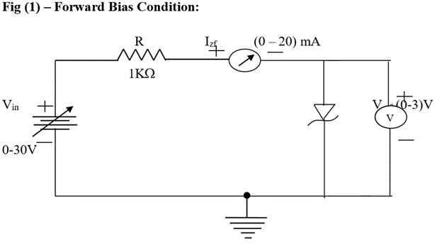
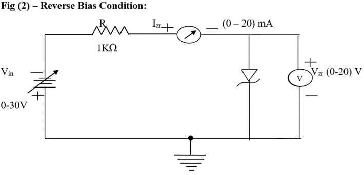
Circuit Diagram:
Procedure:
Forward biased condition:
- Connect the circuit as shown in fig (1).
- Vary VZF gradually steps of 0.1 volts up to 5volts and note down the corresponding readings of IZF.
- Tabulate different forward currents obtained for different forward voltages.
Reverse biased condition:
- Connect the circuit as shown in fig (2).
- Vary VZR gradually in steps of 0.5 volts up to 8 volts and note down the corresponding readings of IZR.
- Tabulate different reverse currents obtained for different reverse voltages.
Observation Table:
Forward biased conditions:
| Sl. No. | Forward Voltage across the diode VZF (volts) | Forward current through the diode IZF (mA) |
Reverse biased conditions:
| Sl. No. | Reverse Voltage across the diode VZR (volts) | Reverse current through the diode IZR (µA) |
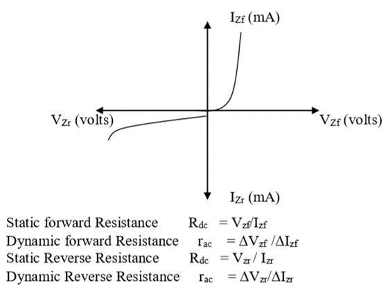
Graph:
- A graph sheet is taken and divided it into 4 equal parts. Origin at the center is marked of the graph sheet.
- Now marked
+ve x-axis as VZF -ve x-axis as VZR +ve y-axis as IZF -ve y-axis as IZR
- The readings tabulated for zener diode forward biased condition in first Quadrant and Zener diodes reverse biased condition in third Quadrant.
Apparatus Used:
| Sl No. | Name of Apparatus | Quantity | Specification | Makers name |
| 1. | Zener Diode characteristics trainer kit | 1 | Zener Breakdown 5.1 V, 6.8 V | M.E.W. |
| 2. | Regulated power supply | 1 | 0 – 30 V DC | M.E.W. |
| 3. | Micro-ammeter | 1 | 0-500 µA, PMMC type |
Precautions:
- While doing the experiment do not exceed the ratings of the diode. This may lead to damage the diode.
- Connect voltmeter and Ammeter in correct polarities as shown in the circuit diagram.
- Do not switch ON the power supply unless you have checked the circuit connections as per the circuit diagram.
Inference:
- In the forward biased mode the zener diode operates as a p-n diode.
- In the reverse biased mode zener diode has large breakdown voltage and though the current increases the voltage remains constant. Thus it acts as a voltage regulator.
Result:
- The zener diode characteristics have been studied.
- The zener breakdown voltage was found to be = ___________
Remarks:
Views: 1328