Experiment No.: 7
Experiment Name:
Testing the proper functioning of power electronic switches – SCR, IGBT, SCS and TRIAC
Objective:
To test SCR, IGBT, SCS and TRIAC.
Theory:
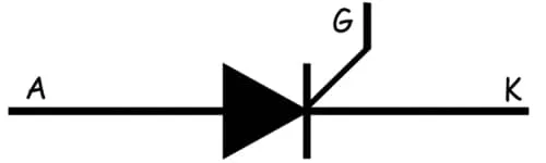
SCR: Silicon Controlled Rectifier (SCR) is a unidirectional semiconductor device made of silicon. This device is the solid state equivalent of thyratron and hence it is also referred to as thyristor or thyroid transistor. In fact, SCR (Silicon Controlled Rectifier) is a trade name given to the thyristor by General Electric Company. Basically, SCR is a three-terminal, four-layer semiconductor device consisting of alternate layers of p-type and n-type material.
Hence it has three pn junctions J1, J2 and J3. The figure below shows an SCR with the layers p-n-p-n. The device has terminals Anode(A), Cathode(K) and the Gate(G). The Gate terminal(G) is attached to the p-layer nearer to the Cathode(K) terminal.

An SCR can be considered as two inter-connected transistors as shown below.
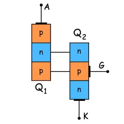
It is seen that a single SCR is the combination of one pnp transistor (Q1) and one npn transistor (Q2). Here, the emitter of Q1 acts as the anode terminal of the SCR while the emitter of Q2 is its cathode. Further, the base of Q1 is connected to the collector of Q2 and the collector of Q1 is connected to the base of Q2. The gate terminal of the SCR is connected to the base of Q2, too.
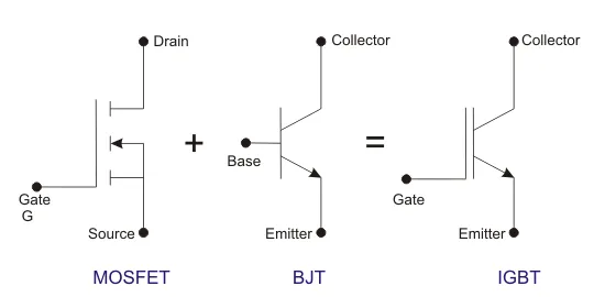
IGBT: Insulated Gate Bipolar Transistor (IGBT) is a relatively new device in power electronics and before the advent of IGBT, Power MOSFETs and Power BJT were common in use in power electronic applications. Both of these devices possessed some advantages and simultaneously some disadvantages. On one hand, we had bad switching performance, low input impedance, secondary breakdown and current controlled Power BJT and on the other we had excellent conduction characteristics of it. Similarly, we had excellent switching characteristics, high input impedance, voltage controlled PMOSFETs, which also had bad conduction characteristics and problematic parasitic diode at higher ratings. Though the unipolar nature of PMOSFETs leads to low switching times, it also leads to high ON-state resistance as the voltage rating increases.
Thus the need was for such a device which had the goodness of both PMOSFETs and Power BJT and this was when IGBT was introduced in around the early 1980s and became very popular among power electronic engineers because of its superior characteristics. IGBT has PMOSFET like input characteristics and Power BJT like output characteristics and hence its symbol is also an amalgamation of the symbols of the two parent devices. The three terminals of IGBT are Gate, Collector and Emitter. The figure below shows the symbol of IGBT.
IGBT is known by various other names also, such as- Metal Oxide Insulated Gate Transistor (MOSIGT), Gain Modulated Field Effect Transistor (GEMFET), Conductively Modulated Field Effect Transistor (COMFET), Insulated Gate Transistor (IGT).
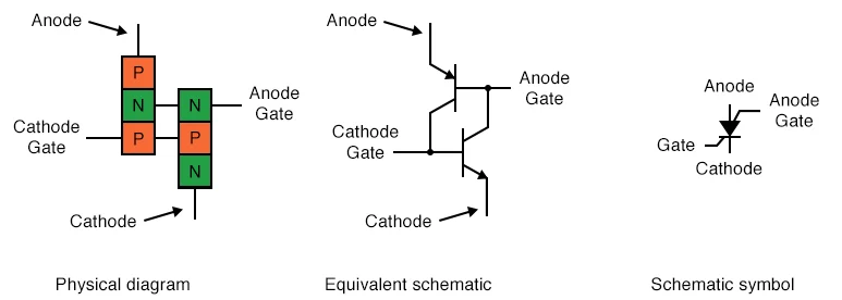
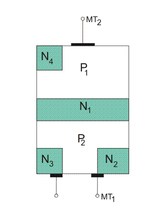
SCS: Silicon controlled switch (SCS), like the SCR, is a unilateral, four layer three junction P-N-P-N silicon device with four electrodes namely cathode C, cathode gate G1, anode gate G2 and the anode A, as shown in figure. Infact, the SCS is a low power device compared with the SCR. It handles currents in milli amperes rather than amperes. SCS differs from an SCR in the following aspects. It has an additional gate—the anode gate.It is physically smaller than SCR.It has smaller leakage and holding currents than SCR.It needs small triggering signals. It gives more uniform triggering characteristics from sample to sample.
The basic structure and schematic symbol of SCS are shown in the figures. It may be fabricated by using either the grown junction technique or the planar technique.
If we take the equivalent circuit of an SCR and add another external terminal, connected to the base of the top transistor and the collector of the bottom transistor, we have a device known as a silicon-controlled-switch, or SCS.
TRIAC: A Triac is defined as a three terminal AC switch which is different from the other silicon controlled rectifiers in the sense that it can conduct in both the directions that is whether the applied gate signal is positive or negative, it will conduct. Thus, this device can be used for AC systems as a switch.
This is a three terminal, four layer, bi-directional semiconductor device that controls AC power. The triac of maximum rating of 16 kw is available in the market. Figure shows the symbol of triac, which has two main terminals MT1 and MT2 connected in inverse parallel and a gate terminal.
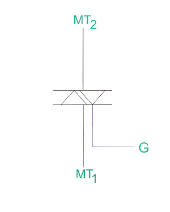
Two SCRs are connected in inverse parallel with gate terminal as common. Gate terminals is connected to both the N and P regions due to which gate signal may be applied which is irrespective of the polarity of the signal. Here, we do not have anode and cathode since it works for both the polarities which means that device is bilateral. It consists of three terminals namely, main terminal 1(MT1), main terminal 2(MT2), and gate terminal G. Figure shows the construction of a triac. There are two main terminals namely MT1 and MT2 and the remaining terminal is gate terminal.
Remarks: The proper functioning of power electronic switches – SCR, IGBT, SCS and TRIAC are tested.
Views: 4940